Papers

13. A Closed Loop In-Plane Movable Suspended Gate FET (CLIP-SGFET) Sensor with a Dynamically Reconfigurable Charge pump
(with Pramod Martha, Ganga K. M., Anju Sebastian and Seena V )
IEEE Sensors Journal, vol. 22 issue 15, Nov. 2022

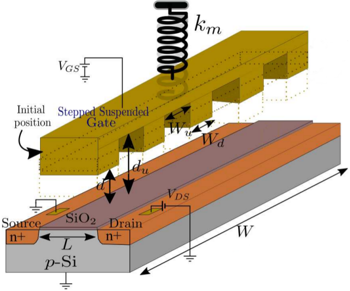
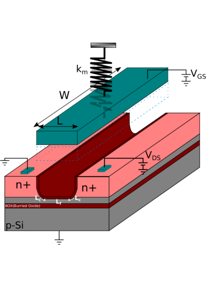
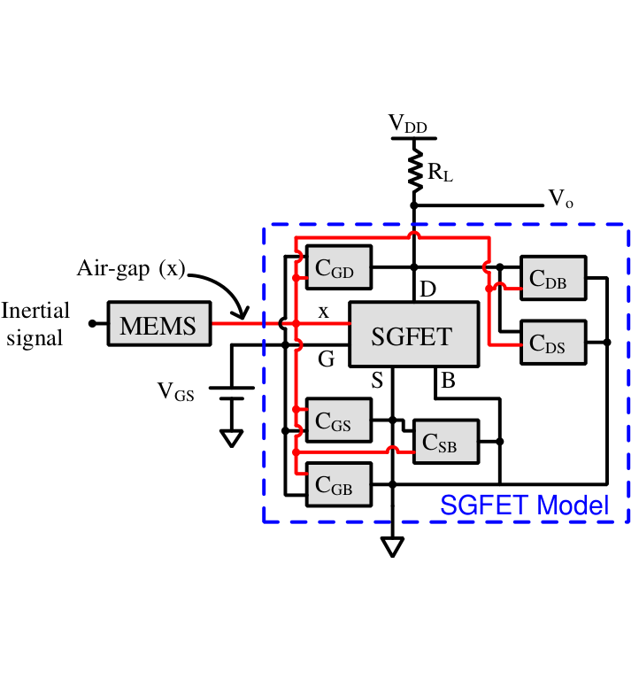
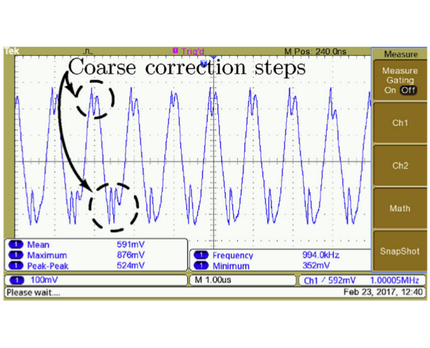
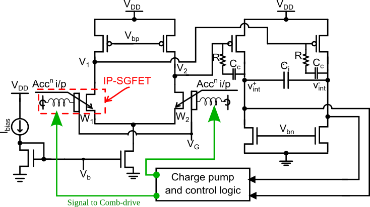
In this paper, we discuss the device, circuit and system design of a closed loop accelerometer sensor using an in-plane movable suspended gate FET. The paper is comprehensive and discusses 
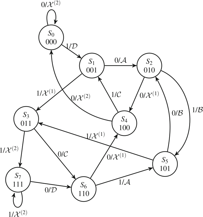
device architecture, simulation methods adopted (we use the Look-up-table method we reported in paper 9 below), circuit design for the sensor, and a suggested fabrication plan for the sensor. 
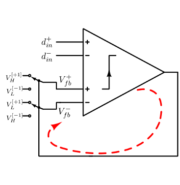
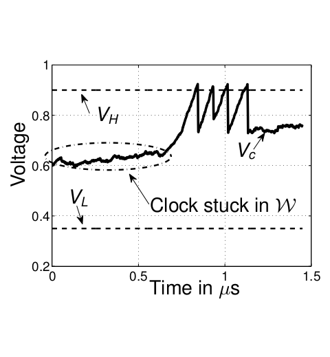
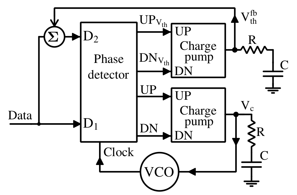
Interface circuits involve novel re-configurable charge pumps for driving actuators in closed loop operation. We use fully differential architecture which requires two charge pumps for generating differential actuator drive along with a high voltage common mode feedback circuit. All circuits are designed in a standard low voltage CMOS process.
--
DOI: https://doi.org/10.1109/TED.2021.3101997

12. A True Time Delay element using cascaded Variable Bandwidth All Pass Filters
(with Mayur Shivamurthy and K.M. Ganga )
International Symposium on Circuits and Systems (ISCAS) 2022

A Gm-C based variable bandwidth all pass filter (APF) as true time delay element is presented in this paper. A cascade of low order APF's is used whose group delay is varied by modulating the Gm of its constituent transconductors. This method avoids the need for high quality varactors, and does not require a large range of capacitance values resulting in design simplicity and reduced power consumption. The proposed design is implemented in TSMC 65 nm technology. Simulation results show that the delay element with 3 stages of third order APF maintains uniform magnitude response with the delayrange-bandwidth product of 0.8 and power/delay-range factor of 0.04 mW/ps upto bandwidth of 1 GHz.

11. CMOS-MEMS Accelerometer with Stepped Suspended Gate FET Array: Design & Analysis
(with Pramod Martha and V. Seena)
IEEE Transactions on Electron Devices, vol. 68 issue 10, Oct. 2021

In this paper we analyze the effect of pull-in instability in out-of-plane movable gate FET based MEMS sensors. Pull-in instability limits the maximum displacement dynamic range of such devices to 1/3rd of the initial air-gap of the transistor. We propose a stepped suspended gate FET sensor that allows increasing the dynamic range up to 50% of the initial airgap, with the same device sensitivity. This also results in a 90% increase in the pull-in voltage. We present the analysis of the stepped-suspended gate FET along with design and simulation of the device.
--
DOI: https://doi.org/10.1109/TED.2021.3101997

10. A CMOS-MEMS Accelerometer with U-channel Suspended Gate SOI FET
(with Pramod Martha and V. Seena)
IEEE Sensors Journal, vol. 21 issue 9.

Suspended gate transistors can be used as inertial sensors, wherein the displacement of the gate relative to the channel can be sensed and used as a measurement of acceleration. In these transistors, the gate is physically far from the channel (few 100's of nm at least) which results in poor gate control over the channel, affecting its performance. This is very similar to short channel effects which happen in scaled MOSFETs. However, unlike MOSFETs for which short channel effects start becoming apparent at lengths of sub 100 nm, for suspended gate FETs these effects are significant even for channel lengths of a few μm due to poor gate control. In this paper, we show how these "Pseudo-short-channel" effects can be reduced by using a U-channel SOI FET.
--
DOI: https://doi.org/10.1109/JSEN.2021.3060186

9. A Technique for Modeling and Simulating Transistor Based MEMS Sensors
(with Pramod Martha, Anju Sebastian and V. Seena)
8th International Symposium on Inertial Sensors & Systems (INERTIAL 2021)

Design of transistor based MEMS sensors (like suspended gate transistors) is quite challenging due to the diverse phenomena involved in their operation. The sensor's output depends on the mechanical structure of the device, the process steps used for the transistor fabrication, and of course - the circuit in which the transistor is used. In this paper, we show how we can design and simulate such a transistor using standard tools for (i) mechanical design, (ii) MOSFET process simulation, (iii) MOSFET device simulation and (iv) circuit simulation; by using a look-up-table model based approach for interfacing the different domain analyses. An example design of an accelerometer sensor with a vertically movable gate transistor is designed and simulated to demonstrate the proposed modeling technique.
--
DOI: https://doi.org/10.1109/INERTIAL51137.2021.9430485

8. Measurements of the effect of jitter on the performance of clock retiming circuits for on-chip interconnects
(with Maryam S. Baghini and Dinesh K. Sharma)
Elsevier Microelectronics Journal Nov. 2018

A new type of clock retiming circuit that performs coarse+fine correction for clock retiming was proposed in Paper #3 below. This paper reports detailed measurements of this circuit quantifying the performance of the same. In particular, the effects of different types of jitter are demonstrated which show the robustness of this circuit. The circuit on which the measurements were performed was fabricated in UMC 130 nm CMOS technology.
--
DOI: https://doi.org/10.1016/j.mejo.2018.09.011

7. Effect of jitter on the settling time of mesochronous clock retiming circuits
(with Amitalok J. Budkuley, Maryam S. Baghini and Dinesh K. Sharma)
Springer, Analog Integrated Circuits and Signal Processing Oct. 2018

A rigorous analyis of the effect of jitter on the settling time of mesochronous clock re-timing circuits is presented in this paper. The dependence of settling time on jitter was first reported by us in Paper #5 below. This dependence was experimentally verified with measurements performed on a test chip. Markov models are developed for different types of jitter and their predictions were verified using simulations in Verilog-A. A few techniques of designing fast settling mesochronous retiming circuits are then presented.
--
DOI: https://doi.org/10.1007/s10470-018-1344-9

6. Sense Amplifier Comparator with Offset Correction for Decision Feedback Equalization based Receivers
(with Dinesh K. Sharma)
Elsevier Microelectronics Journal Dec 2017

In this paper, a decision feedback circuit with integrated offset compensation is proposed. The circuit is built around the sense amplifier comparator. The feedback loop is implemented using a switched capacitor network that picks from one of two pre-computed voltages to be fed back, which results in minimum latency. The circuit was fabricated and tested in 130 nm CMOS.
--
DOI: https://doi.org/10.1016/j.mejo.2017.10.006
Note: A version of this paper is available on Arxiv: https://arxiv.org/abs/1702.01067

5. Settling Time of Mesochronous Clock Re-timing Circuits in the Presence of Timing Jitter
(with Amitalok J. Budkuley and Dinesh K. Sharma)
International Symposium on Circuits and Systems (ISCAS) 2017

In this work, we investigate the effect of timing jitter on the settling time of mesochronous clock re-timing circuits. While the effect of jitter on the BER of synchronizers had been well studied, its effect on settling time had not received attention. The synchronizer system is modeled as a 1 dimensional Markov chain and used to analyze different types of jitter. The paper also proposes techniques of reducing the settling time.
--
DOI: https://doi.org/10.1109/ISCAS.2017.8050694
Note: An extended version of this paper is available on Arxiv: https://arxiv.org/abs/1604.00230

4. Clock Skew Measurement using an All-Digital Sigma-Delta Time to Digital Converter
(with Mahadev G. Shirwaikar and Dinesh K. Sharma)
30th International Conference on VLSI Design 2017

A technique for measuring clock skew between two remote nodes in a chip is reported in this paper. Sub-sampling is used to generate time amplified signals with amplified skew. Since timing variations are typically very slow, this ends up oversampling the skew between the input clocks. Using this oversampling in the converter, a Delta-Sigma Time to Digital converter is constructed. The paper also discusses an all digital implementation of this concept, with negligible penalty in performance.
--
DOI: https://doi.org/10.1109/VLSID.2017.41

3. A Clock Retiming Circuit for Repeaterless Low Swing On-Chip Interconnects
(with Maryam S. Baghini and Dinesh K. Sharma)
30th International Conference on VLSI Design 2017

In this paper we reported a clock retiming circuit for low swing interconnects. The design uses a coarse + fine phase correction scheme. The coarse phase correction is done using a DLL and a control loop that picks the phase closest to the center of the data eye. The fine correction is performed using a VCDL which generates the actual sampling clock. Clock domain transfer from the sampling clock to the receiver clock domain is included in the design. The circuit was fabricated and tested in 130 nm CMOS.
--
DOI: https://doi.org/10.1109/VLSID.2017.12
Note: An extended version of this paper is available on Arxiv: https://arxiv.org/abs/1510.04241

2. Testable Design of Repeaterless Low Swing On-Chip Interconnect
(with Dinesh K. Sharma)
Design Automation and Test in Europe (DATE) 2016

Testability is very important for high volume VLSI designs. Repeaterless low swing interconnects have been shown to be a promising alternative to repeater inserted links for continued interconnect performance scaling. However, these techniques use low swing and mixed signal circuits and their testability is not straightforward. We have reported some simple techniques for testing these mixed signal circuits using techniques established for testing digital circuits, like scan test and BIST with digital I/O's. The fault coverage is evaluated for an example design.
--
Link: http://ieeexplore.ieee.org/document/7459375/
Note: An extended version of this paper is available on Arxiv: https://arxiv.org/abs/1511.06726

1. A Feed Forward Equalizer for Capacitively Coupled On-Chip Interconnect
(with Marshnil Dave, Maryam S. Baghini and Dinesh K. Sharma)
26th International Conference on VLSI Design 2013

This paper reports a 2-tap capacitively coupled feedforward equalizer. A direct coupled weak driver allows arbitrarily low data activity factors. A detailed analysis of the architecture and a fast design method for designing the circuit using worst case sequences is also discussed in the paper.
--
DOI: https://doi.org/10.1109/VLSID.2013.190

Pre-prints

1. Impact of Sampler Offset on Jitter Transfer in Clock and Data Recovery Circuits
(with Maryam S. Baghini and Dinesh K. Sharma)
This paper shows how the input offset of sampling flip-flops in the Alexander phase detector affects the jitter transfer from data to the recovered clock in a clock data recovery circuit. It is shown how the offset of the sampling flip-flop that samples the data at its transitions influences the jitter transfer from data to the recovered clock. Importantly, it is shown that zero offset is not always the best case. The effect is studied for different levels of data dependent jitter. The paper also discusses a tracking circuit that keeps the offset at the minimum jitter point.
--
Link: http://arxiv.org/abs/2001.03553

Patents filed
  • Patent pending: Seena V, A. Sebastian, and N. Kadayinti "Closed loop in-plane movable suspended gate FET based accelerometer and the fabrication method thereof" Indian patent application #202041048333
  • Patent pending: N. Kadayinti and M. Shivamurthy "A circuit for expanding, compressing or delaying a signal." Indian patent application #202041019813